P-N junction Diode
P-N Junction Diode
The P-N junction itself forms the most basic semiconductor device called Semiconductor Diode. Thus semiconductor diode and the P-N junction are one and the same.
The meaning of the term "diode" is the device having "two electrodes" (di-ode).
As shown in Fig. 1 , the diode has two electrodes one each for the two regions on either sides of the junction.


The symbol of a semiconductor diode is as shown in Fig. 2. The two electrodes (terminals) are named as anode and cathode.
The arrowhead in the symbol points in the direction of conventional current through the device.
This current will flow through the diode if and only if an external voltage source is connected to it with appropriate polarities.
Biasing of a P-N Junction Diode
When the P-N junction is formed, the depletion region gets created and the movement of electrons and holes stops. Thus the current flowing through an unbiased P-N junction is zero. To make the current to flow we have to bias the P-N junction diode.
Biasing is the process of applying external DC voltage to the semiconductor diode.
When the external voltage is not applied to the diode, the P-N junction will remain in the state of equilibrium. Therefore there is no current flowing through it.
To make the current to flow, it is necessary to "bias" the diode. The biasing can be of two types:
1. Forward bias. 2. Reverse bias.
Forward Biasing of a P-N Junction Diode
If the p-region (anode) is connected to the positive terminal of the external DC source and n-side (cathode) is connected to the negative terminal of the DC source then the biasing is said to be "forward biasing".
In other words the diode is then said to be forward biased. Generally a resistance is connected in series with the diode to limit the current flowing through it.
Forward biasing of a diode is as shown in Fig. 3 and the symbolic representation is as shown in Fig. 4. The current "If" is a conventional current that flows in the circuit due to the forward biasing.


Operation of a forward biased diode
Due to the negative terminal of external source connected to the n-region, free electrons from n-side are pushed towards the p-side. Similarly the positive end of the supply will push holes from p-side towards the n-side.
With increase in the external supply voltage V, more and more number of holes (p-side) and electrons (n-side) start travelling towards the junction as shown in Fig. 3 and 4
The holes will start converting the negative ions into neutral atoms and the electrons will convert the positive ions into neutral atoms. As a result of this, the width of depletion region will reduce.

Fig. 5 : The effect of increased forward bias on the depletion region and barrier potential
Due to reduction in the depletion region width, the barrier potential will also reduce. Eventually at a particular value of V the depletion region will collapse. Now there is absolutely no opposition to the flow of electrons and holes.
Hence a large number of electrons and holes (majority carriers) can cross the junction under the influence of externally connected DC voltage.
The large numbers of majority carriers crossing the junction constitute a current called as the forward current. The current flow shown in Fig. 6 is the electron current, which is in the opposite direction to that of a conventional current.

Effect of forward bias on the width of depletion region: With increase in the forward bias, the width of the depletion region decreases and so does the barrier potential
Current flow in forward biased diode
As soon as the free electrons enter into the p- region from the n-side, they become valence electrons. So these electrons will jump from one atom to the other to fill up the holes present there.
Thus movement of electrons on p-side will be due to the movement of holes.
These electrons move towards the positive end of the source and the holes will move towards the junction.
Thus current through the p-region flows due to the movement of majority carriers.
Similarly current on the n-side is due to the movement of free electrons, which are the majority carriers.
Hence we can conclude that:
The forward current through a P-N junction diode flows due to the majority carriers and its direction of flow (conventional) is always from anode to cathode.
Forward resistance of diode
The forward current of a diode (Ip) is the current flowing through the forward biased diode which flows due to the majority carriers. Hence If is of the order of few mA.
Due to large current, the forward resistance of the diode is very small. Typically it is of the order of few ohms (10 to 100 ohm).
Voltage Drop Across the Forward Biased Diode (VF)
A Silicon p-n junction has a barrier potential of 0.7 V with the polarity which opposes the external forward voltage. The external voltage needs to exceed 0.7 V so as to initiate conduction.
As soon as the applied external voltage overcomes the barrier potential, the currents starts flowing.
There is a potential drop across the conducting forward biased diode, which has opposite polarities to the barrier potential but has a magnitude which is approximately equal to the barrier potential.
The forward voltage drop is denoted by VF as shown in Fig. 7 and equal to 0.7 V for silicon diode and 0.3 V for Germanium diode.

Fig 7 : Forward voltage drop
The forward voltage drop Vf is due to two factors namely the drop due to barrier potential and drop due to internal resistance Rf.
Reverse Biasing a Diode
If the p-region of a diode is connected to the negative terminal of the external DC supply and n- region is connected to the positive terminal of the DC supply as shown in Fig. 8 then a diode is said to be "reverse biased".
Fig. 8 shows the reverse biasing schematically. The reverse current is denoted by Is and it flows from the cathode to anode of the diode.
Thus reverse current flows exactly in the opposite direction to that of the forward current.
Resistance R is connected to limit the reverse current

Operation of a reverse biased diode
When a diode is reverse biased, holes in the p- region are attracted towards the negative terminal of the supply and electrons on the n-side are attracted towards the positive terminal of the supply as shown in Fig. 9
Widening of depletion region : Due to the movement of electrons and holes away from the junction, width of the depletion region increases as shown in Fig. 9. This happens due to the
creation of more number of positive and negative immobile ions.
Increase in barrier potential : Due to more number of ions present on opposite sides of the junction, the barrier potential or junction potential will increase.
The process of widening of depletion region does not continue for a long time, because there is no steady flow of holes from right to left i.e. from the n-side to p-side.

Fig. 9 : Operation of reverse biased diode
Current flow in the reverse biased diode ( Reverse saturation current)
We know that the p-region consists of a small number of electrons and the n-region contains a small number of holes. These are the minority carriers which are generated thermally.
The minority electrons in the p-region are attracted by the ive end of the dc supply. Hence these electrons will cross the junction and constitute the reverse current Is of the diode. This is shown in Fig. 10
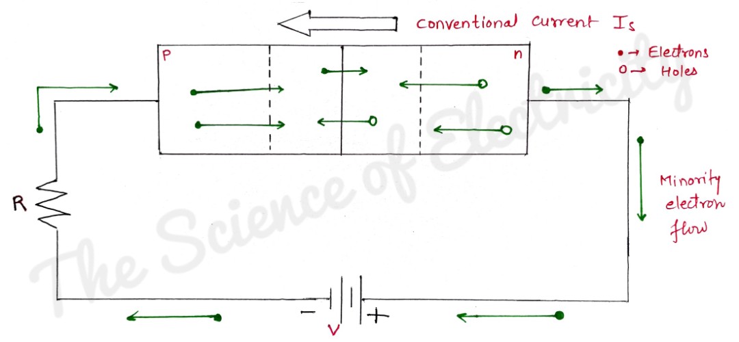
Fig. 10 : Current flow in reverse biased diode
The reverse current is also called as the "Reverse saturation current". As this current is due to the minority carriers, it is small in amplitude. Typically a few uA for germanium diodes and few nanoamperes for the silicon diode.
The reverse saturation current depends on the temperature. It doubles its value for every rise in temperature. Hence at a constant temperature the reverse saturation current
remains constant independent of the reverse voltage.
Reverse current flows due to minority carriers which exist due to elevated temperatures. Hence reverse current is dependent on temperature.
Important points about the reverse current
1. It flows from cathode to anode.
2. It flows due to minority carriers.
3. Its value is much smaller than that of the forward current.
4. It is independent of reverse voltage but dependent on the temperature.
Resistance of reverse biased diode
The reverse current is small which indicates that the resistance offered by a reverse biased diode is very large. It is denoted by R, and its value is a few hundred kilo ohm.
Voltage across reverse biased diode
The reverse biased diode is equivalent to a large value resistor. It forms a potential divider with the current limiting resistance R, across the external voltage V, as shown in Fig. 11

Fig. 11 : Voltage across reverse biased
Thus the reverse voltage is approximately equal to the applied voltage and its polarity is as shown in Fig. 11
Since the polarity of VR is opposite to the polarity of V., the reverse voltage is treated as a negative voltage.
Breakdown in the Reverse Biased Diode
The reverse saturation current flowing in the reverse biased diode is dependent only on the temperature and independent of the reverse voltage applied externally. However now we are going to learn the phenomenon called reverse breakdown which takes
place at a large reverse voltage. The breakdown in a reverse biased diode can take place due to the following effects :
1. Avalanche effect and 2. Zener effect.
Breakdown due to the avalanche effect
When a very large reverse voltage is applied to a diode the events take place in the following sequence :
Due to large reverse voltage the velocity of the minority carriers will increase to a great extent. Therefore the kinetic energy associated with them will also increase.
While travelling, these minority carriers will collide with the stationary atoms and impart some of the kinetic energy to the valence electrons present in the covalent bonds.
Due to this additionally acquired energy, these valence electrons will break the covalent bonds and jump into the conduction band to become free for conduction.
Now these free electrons will be accelerated and they knock out some more valence electrons by means of collisions. This "chain reaction" is called as "Avalanche effect".
In a very short time, a large number of free minority electrons will be available for conduction and a large reverse current will flow through the reverse biased diode. The avalanche breakdown has thus taken place.
Why should we avoid breakdown ?
At the time of the avalanche breakdown, a large reverse voltage appears across the diode and a large reverse current flows through it.
Therefore a large power gets dissipated in the diode. The junction temperature of the diode may exceed its safe limits and the diode will be damaged permanently.
Therefore, the reverse breakdown should always be avoided.
Breakdown due to the zener effect
The reverse breakdown can take place due to another effect called zener effect. The events take place in the following sequence in the process of breakdown due to zener effect :
Due to the heavy doping of p and n-sides of the diode, the depletion region is narrow in the reverse biased condition. All the reverse voltage V appears across the depletion region. Therefore the electric field which is the voltage per unit distance is very intense across the depletion region. This intense electric field can pull some of the valence electrons by breaking the covalent bonds. These electrons then become free electrons. A large number of such electrons can constitute a large reverse current through the diode. This is called as the breakdown due to zener effect.
Does the breakdown always damage the diode?
The answer is no. If we use the external current limiting resistance such that the reverse current at the time of breakdown is kept at a low value, then the power dissipation taking place in the diode will be well below the dangerous level and the diode does not get damaged.
But otherwise the diode cannot sustain the breakdown and it will be damaged permanently.


Comments
Post a Comment