Semiconductor Theory
Semiconductors
Definition :
The materials, whose electrical
conductivity lies between those of conductors and insulators and have negative
temperature coefficient of resistance, are known as semiconductors.
Semiconductor Materials :
The few examples of semiconductor
materials are as under :
1.Carbon (C)
2. Silicon (Si)
3.Germanium (Ge)
4. Selenium (Se)
5.Gallium Arsenide (GaAs)
6.Cadmium Sulphide (CdS).
The commonly used semiconductor materials are Germanium and Silicon. These are tetravalent elements i.e. materials having four valency.
Atomic Structures of Germanium
and Silicon :
(i) Atomic structure of Germanium and Silicon atoms :
Fig. 1.3 (b) shows the atomic structure of a Germanium atom in which first, second, third and fourth orbits have 2, 8, 18 and 4 electrons respectively, with the result that the atomic number for Germanium is 32.
Fig. 1.3 (a) shows the atomic structure of a Silicon atom in which first, second and third orbits have 2, 8, and 4 electrons respectively, with the result that the atomic number for Silicon is 14.

(ii) Atomic structure of
Germanium and Silicon crystals:
Fig. 1.4 shows a simplified two-dimensional representation of crystalline structure of Germanium or Silicon crystal. Each Germanium atom is surrounded by 4 neighbouring Germanium atoms and each atom has 4 valence electrons. The core represents the nucleus and filled orbits, At absolute zero, all the valence electrons are tightly bound to the nucleus of the parent atoms and hence no free electrons are available for electrical conduction.

Fig. 2: Atomic
structure of Ge and Si crystals
Classification of Semiconductors
:
The classification of
semiconductors is as under:
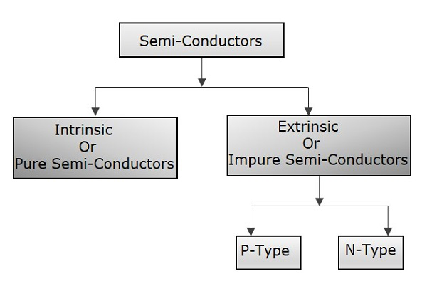
Fig. 3: Classification of Semiconductors
Types of Semiconductors :
The semiconductors are of the following two types :
1. Intrinsic semiconductor.
2.
Extrinsic semiconductors.
1. Intrinsic Semiconductors :
Definition :
A semiconductor in an extremely pure form (Le. without any impurity) is known as an intrinsic semiconductor. Conduction of Current

Fig. 4: Conduction of current in an intrinsic semiconductor
When electric field Vs is applied across an intrinsic semiconductor, the current conduction takes place due to free electrons and holes.
The free electrons are generated due to the breaking up some covalent bonds by thermal agitation (or energy). At the same time, the same number of holes are created in the covalent bonds.
The free electrons drift towards the positive terminal of the battery Vs and the holes towards the negative terminal.
This movement of charge carriers constitute the electric current I under the influence of electric field Vb and it flows through the intrinsic semiconductor.
Since the electrons are negatively charged, the direction of electric current (conventional) I is opposite to the direction of their motion of free electrons and in the direction of holes.
The two types of charge carriers i.e. free electrons and holes move in opposite direction.
When the flow of charge carriers is due to an applied voltage (as shown in Fig. 1.6), the resultant current is called a drift current.
A second type of current may also exist in an intrinsic semiconductor. This current is called diffusion current and it flows as a result of a gradient of carrier concentration (i.e. the difference in carrier concentration from one region to another).
The diffusion current may also be due to the motion of both free electrons and holes.
4. Extrinsic Semiconductors:
Definition :
As the intrinsic semiconductor materials have negligible and poor conductivity at room temperature, it is not useful for practical applications of electronics.
For improving the electrical conductivity of intrinsic semiconductor, certain amount of desired impurity atoms are to be added into it to make the imbalance of free electrons and holes. They are called dopands.
The intrinsic semiconductor containing small amount of desired impurity atoms is known as an extrinsic semiconductor. It is also defined as a doped intrinsic semiconductor.
The impure form of a semiconductor is known as an extrinsic semiconductor.
Doping :
The process of deliberately
adding or diffusing impurity atoms to the intrinsic semiconductor crystal is
called doping.
The purpose of adding impurity is to increase either the number of free electrons or holes in the semiconductor crystal i.e. to increase the conductivity of intrinsic semiconductors.
Types of Impurity Elements :
To increase the conductivity of the intrinsic semiconductor, trivalent or pentavalent impurity elements are doped to it.
There are two types of impurity elements, namely trivalent and pentavalent.
(1) Trivalent (Acceptor) impurity elements:
The impurity elements that accept the free electrons from the intrinsic semiconductor is called trivalent impurity elements. These are third group elements.
Typical examples are Boron (B),
Gallium (Ga), Aluminium (Al) and Indium (In).
These impurities are also called
acceptor impurities because the holes created have affinity to accept free
electrons.
(2) Pentavalent (Donor) impurity elements :
The impurity element that provides (or donates) excess of free electrons to the intrinsic semiconductor is called pentavalent impurity elements. These are pentavalent group elements.
Typical examples are Phosphorus
(P), Arsenic (As) and Antimony (Sb).
These impurities are also called
donor impurities because these impurities donate or provide excess of free
electrons.
Types of Extrinsic Semiconductors
:
The extrinsic semiconductors are
of the following two types :
1. P-type semiconductors.
2. N-type semiconductors.
P-type Semiconductor:
Definition :
When a small amount of trivalent
(acceptor) impurity is added to the intrinsic semiconductor, then it is known
as P-type semiconductor.
The P-type semiconductor is formed by adding a small amount of trivalent/(Boron, Gallium or Aluminium) impurity element to the intrinsic semiconductor (pure Silicon or Germanium) material which acts as a base material.
The addition of trivalent impurity
provides a large number of holes in the intrinsic semiconductor.
Working Principle :
- Consider the structure of a P-type semiconductor as shown in Fig.
- The Boron atom in the crystal has only 3 valence electrons.
- Each Boron atom is surrounded by 4 neighbouring Germanium (or Silicon) atoms.
- Three valence electrons of Boron atom share with the 3 electrons of 3 neighbouring Germanium atoms forming 3 covalent bonds.
- The fourth neighbouring Germanium atom is unable to form a covalent bond with Boron atom, because Boron atom does pot
- have fourth electron in its valence orbit.
- The fourth covalent bond remains incomplete for want of fourth electron in Boron atom. This deficit of one electron in the Boron atom gives rise to a hole.
- The number of holes generated in the Germanium crystal depends upon the amount of Boron atoms added to the crystal
- The hole has a great tendency to snatch valence electron from the neighbouring atom to form a covalent bond
- This tendency is so great that an electron in an adjacent covalent bond, having very small additional energy can jump to occupy the vacant position.
- This electron then completes the covalent bond around all the Boron atom.
- At room temperature, the thermal energy is sufficient to provide this energy so as to fill the incomplete bond around all Boron atoms.
- To make up the fourth covalent bond, Boron atom takes one electron from the neighbouring Germanium atom by breaking a covalent bond. Now two things happen.
- A vacancy is created in the adjacent covalent bond from where the electron had jumped. This vacancy has a positive charge associated with it, hence, it is a hole as shown in Fig. 1.7 (b).
- Due to the filling of the incomplete fourth covalent bond around the Boron atom, it now becomes a negative ion.
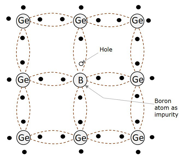
Fig. 5: P-type semiconductor
- At absolute zero temperature, there is no movement of electrons and holes due to zero thermal energy.
- Hence P-type semiconductor behaves as a perfect insulator at absolute zero temperature.
- At room temperature, some of the covalent bonds may get broken, because of thermal energy.
- This gives rise to electron-hole pairs. These holes add to the existing holes.
- There exist a large number of holes (i.e. positively charged carriers).
- In P-type semiconductor, holes are majority carriers, whereas free electrons are minority carriers.
- In energy band diagram, Fermi level is nearer to the valence band.
N-type Semiconductor :
Definition :
When a small amount of pentavalent (donor) impurity is added to the intrinsic semiconductor, then it is known as N-type semiconductor.
- The N-type semiconductor is formed by adding a small amount of pentavalent impurity (Phosphorus or Arsenic or Antimony) to the intrinsic semiconductor (pure Silicon or Germanium) material which acts as a base material.
- The addition of pentavalent impurity provides a large number of electrons in the intrinsic semiconductor.
Working Principle :
- Consider the structure of an N-type semiconductor as shown in Fig. 1.8.
- The fifth valence electron of Phosphorus atom finds no place in the covalent bond and is unable to form a covalent bond with Germanium atom for want of an additional electron in their orbit.
- Since it is not associated with any covalent bond and is quite far from the nucleus, it is very loosely bound. It requires very little energy to free itself from the attractive force of its nucleus.
- The Phosphorus atom in the crystal has only five valence electrons.
- Each Phosphorus atom is surrounded by 4 neighbouring Germanium (or silicon) atoms.

- This Phosphorus atom fits in the Ge (or Si) crystal in such a way that its 4 valence electrons share with the 4 valence electrons of 4 different neighbouring (or adjacent) Germanium atoms forming 4 covalent bonds with these Germanium atoms.
- At absolute zero temperature, there is no movement of electrons and holes due to zero thermal energy.
- The additional energy required to detach the fifth valence electron from its nucleus is so small that at room temperature practically all such electrons become free.
- At room temperature, all those donated electrons acquire sufficient thermal energy and become detached from its nucleus.
- It then becomes free to move anywhere within the crystal.
- At the time when this electron has become free from the Phosphorus atom, the remaining atom becomes a positive ion.
- The number of thermally generated electron-hole pairs will be very small compared to the number of free electrons donated by impurity atoms.
- Consequently, the concentration of holes is much less than free electrons in its intrinsic value.
- In N-type semiconductor, free electrons are majority carriers, whereas holes are minority carriers.
- In energy band diagram/Fermi level is nearer to the conduction band.
- Thus N-type semiconductor behaves as a perfect insulator at absolute zero temperature.
Comparison of Intrinsic and
Extrinsic Semiconductors:
|
Intrinsic
Semiconductor |
Extrinsic
Semiconductor |
|
1. It is an
extremely pure form of semiconductor. |
1. It is a
doped semiconductor. |
|
2. The number
of free electrons and holes generated due to thermal energy are equal. |
2.The number
of free electrons and holes generated due to thermal energy
are not equal. |
|
3. The current
conduction is due to free electrons and holes. |
3. The major
part of current conduction is due to majority carriers, either holes or free
electrons. |
|
4. The Fermi
level is at the centre of forbidden energy gap and is unchanged with change in temperature. |
4.The Fermi
level shifts upward or downward as per doping material and
with change in temperature. |
|
5. The
electrical conductivity is very poor at room temperature. |
5. The
electrical conductivity is comparatively high at room temperature. |
|
6. It is less
useful. |
6. More
useful. |
|
7. It has no
further types. |
7. It is of
two types: (a) P-type, (b) N-type. |
Source of Images :- Google


Nice answer
ReplyDeleteThank you
Delete